
Chiplet Ecosystem Standardization: UCIe Alliance’s 2026 Milestones
By 2026, it has become clear that the future of advanced encapsulation and heterogeneous integration will be defined as much by standards as by process technology. Universal Chiplet Interconnect Express, or UCIe, sits at the center of this transformation. Launched as an open die-to-die interconnect specification for chiplets, the UCIe Alliance has now accumulated several generations of specifications and ecosystem deliverables that are reshaping how the industry thinks about system design, advanced packaging, and multi-vendor chiplet interoperability.

The 2026 milestones of the UCIe Alliance are not just incremental updates to a protocol. They mark a maturation point for the entire chiplet ecosystem: from isolated proprietary multi-die implementations to a more open, standardized, and scalable model. This shift directly impacts advanced encapsulation techniques, 2.5D and 3D integration, and the way heterogeneous systems are assembled within a package. For designers, integrators, and packaging engineers, understanding what these milestones mean is essential to navigating the next wave of semiconductor innovation.
From Custom Multi-Die to Open Chiplets
In the early days of multi-die systems, advanced packaging was mostly a bespoke endeavor. Each company defined its own die-to-die signaling schemes, mechanical constraints, test flows, and management interfaces. While this delivered impressive products, it came at the cost of ecosystem fragmentation. Integrating dies from different vendors was difficult or impossible, and each design cycle recreated many of the same integration challenges.
UCIe was created to break this pattern. The Alliance’s goal is a standardized die-to-die interface that covers the physical layer, link layer, protocol mapping, and software model needed to mix and match chiplets from multiple vendors in a single package. At its core, UCIe defines a common electrical and logical language for chiplets, leveraging well-established protocols such as PCI Express and Compute Express Link for higher-level communication while providing a dedicated, efficient physical interface optimized for in-package connections. This framework turns advanced encapsulation and heterogeneous integration into repeatable, interoperable practices rather than one-off engineering feats.
UCIe Generations: Setting the Stage
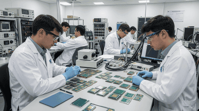
By 2026, UCIe has progressed through several specification generations, each expanding its scope and performance. The initial releases focused on a robust die-to-die physical and link layer alongside mappings for standard protocols, enabling early adopters to implement multi-die systems with consistent electrical and logical behavior. Subsequent versions added refinements in reliability, usage models, and support for different packaging cost points, making the standard more attractive for automotive and cost-sensitive markets.
Later revisions introduced more ambitious capabilities. Support for comprehensive system architecture and lifecycle management of multi-chip packages brought test, debug, and in-field telemetry under a standardized umbrella. Crucially, the specification expanded into 3D packaging, defining modes optimized for hybrid bonding and fine-pitch vertical interconnects. This progression set the foundation for the 2026 milestones: a UCIe stack that can scale across 2D, 2.5D, and 3D advanced encapsulation approaches, while delivering ever higher bandwidth density, lower power per bit, and stronger system-level manageability.
Advanced Encapsulation Meets Standardization
Advanced encapsulation is no longer just about protecting and connecting a single monolithic die. For a chiplet-based system, the package is the platform on which the entire system is assembled. Interposers, redistribution layers, micro-bumps, hybrid bonds, underfill materials, and thermal interfaces all come together to realize a dense, high-performance multi-die module. UCIe provides the digital and protocol skeleton that allows these physical elements to be used in a predictable, interoperable way.
With a standardized die-to-die interface, encapsulation engineers can design package architectures knowing that certain electrical and mechanical parameters will be common across chiplets. Bump pitches, routing constraints, power delivery zones, and thermal paths can be optimized around known link characteristics rather than proprietary, shifting targets. This reduces design risk, simplifies verification, and enables more modular package designs where chiplets can be swapped or upgraded without redesigning the entire encapsulation structure.
Heterogeneous Integration as a Design Principle
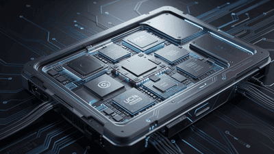
Heterogeneous integration has moved from a niche capability to a mainstream design principle. Instead of forcing all functionality onto a single bleeding-edge process node, designers can split the system into chiplets: high-performance logic on the most advanced node, memory interfaces and I/O on intermediate nodes, and analog, RF, or power management on mature nodes. This approach can improve yield, cost, and time-to-market while enabling a rich mix of capabilities.
UCIe’s layered architecture is designed explicitly to support this heterogeneity. The physical and link layers focus on robust, high-speed connectivity, while the protocol layers allow chiplets to carry familiar traffic such as PCIe and CXL, or custom raw mode data for specialized use cases. As a result, multiple chiplets built on different process technologies, by different vendors, and for different roles can coexist in a single system-in-package. Advanced encapsulation technologies, including 2.5D interposer-based and 3D hybrid-bonded stacks, become the mechanical and electrical fabric that realizes this heterogeneous system.
Milestone: Performance and Bandwidth Density
One of the most visible aspects of the UCIe roadmap is the steady climb in data rates and bandwidth density. Early implementations already surpassed traditional board-level interfaces by taking advantage of short, in-package channels. Later revisions pushed data rates further while keeping an eye on power efficiency and signal integrity. By the time the Alliance delivered its 2026 milestones, the standard supported multi-tens of gigatransfers per second per lane, doubling the bandwidth of earlier specifications and significantly increasing the throughput available within a package.
This performance trajectory is essential for advanced encapsulation and heterogeneous integration. Large AI accelerators, high performance CPUs, and network processors increasingly rely on chiplet-based architectures with extensive on-package communication. Whether connecting compute tiles to shared last-level cache, tying together memory chiplets in a NUMA-style configuration, or linking specialized accelerators, high bandwidth density at the package level is a necessity. The UCIe Alliance’s achievements in data rate, signaling robustness, and power optimization enable encapsulation engineers to design packages that carry enormous data volumes without resorting to exotic or proprietary interconnect schemes.
Milestone: 3D Integration and UCIe-3D

A critical 2026 milestone lies in the formalization and refinement of UCIe support for 3D integration. While early chiplet systems largely used side-by-side placement on an interposer or organic substrate, the industry is now moving toward vertical stacking. UCIe-3D modes are designed for environments where chiplets are connected through through-silicon vias or, more prominently, hybrid bonding with micro or even sub-micron pitch.
This 3D support has several implications for advanced encapsulation. Packages must manage tighter thermal coupling between layers, more complex power delivery paths, and new reliability concerns related to vertical interconnects. By standardizing how die-to-die links behave in these 3D environments, UCIe helps ensure that chiplets designed by different companies can be stacked safely and efficiently. It also gives packaging teams a consistent framework for material selection, mechanical design, and test strategies, reducing the risk associated with pioneering 3D multi-die stacks.
Milestone: System Manageability and DFx
Another major step forward in the UCIe Alliance’s 2026 achievements is the emphasis on manageability and design-for-everything (DFx) across the entire system-in-package lifecycle. As chiplet counts grow and packages become more complex, system-level observability and control are just as important as raw bandwidth. Standards now encompass features for unified test access, telemetry, error reporting, and debug across multiple chiplets.
From an encapsulation and heterogeneous integration perspective, this system manageability layer is transformative. It allows manufacturers and field operators to monitor thermal hotspots, link health, and error rates across the entire package. It supports predictive failure analysis, which is especially important in automotive and other safety-critical domains where advanced packaging is increasingly adopted. Encapsulation no longer ends at the physical boundaries of the mold compound; it includes a digital nervous system that can report on the health of the multi-die assembly over its lifetime.
Milestone: Broader Usage Models and Market Adoption
The 2026 milestones also reflect a widening of UCIe’s usage models. What began as a high performance computing and data center focused initiative has expanded into consumer, networking, and automotive use cases. Refinements in reliability, extended environmental specifications, and cost-optimized packaging options enable UCIe-compliant chiplets to appear in a broader range of products. Standardized encapsulation and integration flows mean that lessons learned in one market segment can carry over to others more readily.
This broader deployment feeds back into the packaging supply chain. OSATs and foundries can justify larger investments in UCIe-capable lines, equipment, and test capabilities when there is a diversified customer base. Encapsulation service providers can develop reference flows for UCIe chiplets, reducing custom engineering effort and speeding time-to-market. As more products rely on standardized chiplet interfaces, the entire advanced packaging ecosystem gains economies of scale and a common language for integration.
Implications for Advanced Encapsulation Flows
For practitioners in advanced encapsulation, the UCIe Alliance’s 2026 achievements bring both opportunities and new design constraints. On the opportunity side, standardized die-to-die interfaces unlock modular package construction. Instead of designing a unique encapsulation for every system, engineers can create platform packages that support families of chiplets, swapping and upgrading them as requirements evolve. This can simplify portfolio management and enable longer-lived package platforms.
On the constraint side, adherence to UCIe specifications imposes certain rules on bump layout, power delivery, routing density, and mechanical design. Design teams must coordinate early with chiplet designers to ensure that physical interfaces and package plans align with the standard while still meeting product-specific goals. Thermal and mechanical simulations must account for UCIe channel requirements, such as maximum trace lengths and impedance targets. The payoff is that once these constraints are satisfied, interoperability and reuse become much easier to achieve.
Design Strategies in a UCIe-Centric Ecosystem
System architects now have to think in “chiplet-native” terms. Rather than asking how big a monolithic SoC can be, they ask how functionality should be partitioned across chiplets. UCIe’s standardized interconnect encourages designs where compute tiles, cache blocks, IO hubs, and specialized accelerators are separate but tightly linked dies. Advanced encapsulation technologies then determine whether these chiplets live side-by-side on an interposer, in a fan-out package, or stacked vertically.
A key design strategy is to separate performance-critical paths, which may demand the fastest and most power-efficient UCIe links, from less demanding connections that can use slower modes or other interfaces. Encapsulation engineers work with architects to decide which chiplets must be physically closest, which layers need the best cooling, and how power should be distributed. UCIe provides a predictable communication fabric across these decisions, so that the package acts as a coherent, high-performance system rather than a loose collection of parts.
Impact on Supply Chain and Ecosystem Dynamics
Standardization changes how the supply chain operates. In a UCIe-centric world, a chiplet vendor does not need to negotiate a one-off electrical interface with each system integrator. Instead, compliance with the specification and associated test suites becomes the baseline. OSATs and foundries can invest in common test boards, fixtures, and characterization methodologies. This lowers barriers for new entrants in the chiplet market and encourages specialization: some companies focus on world-class memory chiplets, others on AI accelerators, others on mixed-signal peripheral tiles.
For advanced encapsulation houses, these dynamics mean that new business models become viable. A provider can position itself as a “system-in-package integrator,” assembling UCIe-compliant chiplets from multiple vendors into custom modules. The standardized interface allows the integrator to qualify chiplets and flows once and reuse that knowledge across projects. Over time, this could lead to catalogues of reference designs, where customers pick chiplets and encapsulation options like building blocks to rapidly prototype and deploy heterogeneous systems.
Challenges that Remain
Despite the impressive progress marked by the UCIe Alliance’s 2026 milestones, several challenges remain in marrying standardization with the realities of advanced encapsulation and heterogeneous integration. One challenge is ensuring robust interoperability across the full range of process technologies, packaging types, and use cases. Subtle variations in signal integrity, power noise, or thermal behavior can still cause issues that standards alone cannot fully eliminate.
Another challenge is maintaining flexibility for innovation. While standards provide a stable foundation, they can also risk constraining new ideas if they become too rigid. The UCIe ecosystem must balance backward compatibility with the need to embrace emerging packaging technologies, such as new 3D bonding methods, novel materials, or radically different architectural approaches. The Alliance’s work on multi-generation compatibility and extensible feature sets is an attempt to strike that balance, but real-world products will test how well it holds.
Looking Ahead: UCIe and the Next Wave of Heterogeneous Systems
The story does not end in 2026. As compute demands continue to rise, particularly driven by AI, data analytics, and edge applications, chiplet-based systems will grow in both scale and complexity. We can expect more tiers of memory, more specialized accelerators, and tighter integration between compute, storage, and networking within a single encapsulated module. Advanced encapsulation will increasingly resemble the design of circuit boards and systems, just at a far smaller scale and with much higher integration density.
UCIe is poised to be the backbone of this evolution. Future extensions are likely to focus on even higher data rates, finer integration with 3D stacking methodologies, and more sophisticated manageability and security capabilities. For designers, the key will be to treat UCIe and advanced encapsulation not as separate concerns, but as two sides of the same coin. The package is the system, and the system is defined by standardized connectivity, robust encapsulation, and carefully orchestrated heterogeneous integration.
Conclusion: From Physical Packages to Standardized Platforms
The UCIe Alliance’s 2026 milestones mark a turning point in how the industry views advanced encapsulation and heterogeneous integration. What used to be custom, proprietary, and difficult to reuse is becoming standardized, modular, and ecosystem-driven. Chiplets, once an internal implementation detail of a single vendor’s product line, are evolving into standardized components that can be integrated across companies and markets.
For practitioners in packaging, system design, and semiconductor strategy, the message is clear. Mastery of advanced encapsulation techniques must be complemented by a deep understanding of the UCIe standard and the chiplet ecosystem it enables. Together, they transform the package from a protective shell into a programmable platform, where heterogeneous functions, processes, and vendors come together to build systems that would be impossible as monolithic devices. The 2026 milestones are a waypoint on this journey, but they already signal a profound redefinition of what it means to design and build a chip in the era of standardized chiplet ecosystems.





